Calculation of the electronic and optical properties of an AlGaN/GaN LED diode
In this application, we show a 1D calculation of quantum and optical properties of a AlGaN/GaN LED diode with three GaN quantum wells.
The simulated structure is the following:
After a buffer n-doped AlGaN layer, a Al0.78InN barrier layer is present, then a series of three AlGaN/GaN quantum wells, each 2 nm-wide, followed by a p-doped AlGaN layer.
In this wurtzite nitride heterostructure, strain and strain induced piezoelectric polarization play a fundamental role in the description of the electronic properties. In fact, on one hand, effects of strain on the conduction and band profiles have to be taken in account through the appropriate k.p model and, on the other hand, the piezoelectric polarization term, together with the spontaneous polarization one, have to be included in the Poisson-Drift-Diffusion calculations.
Thus, first of all, strain and polarization fields are calculated.
Strain maps are obtained by defining the AlGaN substrate as the reference material.
Then, a simulation model for drift-diffusion calculation is defined, which includes physical models for srh recombination and direct (radiative) recombination. An increasing bias is applied to the diode until conduction regime is reached.
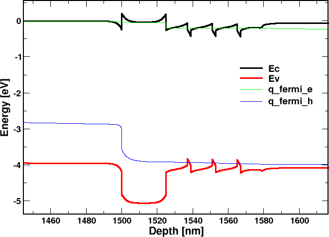
These are the conduction and valence band profiles we obtain for an applied bias Vb=4 V; quasi-fermi levels for electrons and holes are indicated, showing that the three GaN quantum wells levels are populated both in conduction and in valence band.

1. Quantum properties
top
Schroedinger equation is solved, with an EFA model: a single-band model for conduction band and 6x6 k.p model for valence bands.
Eigenvalues and eigenfunctions are calculated to get energy levels and wavefunctions in the three quantum wells: 20 eigenstates are obtained.
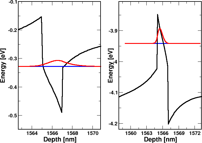
Here are the first conduction band state (left) and the first valence band state (right) in the third quantum well.

2. Optical properties
top
The k.p optical matrix elements are calculated and used to find the optical spectrum of the spontaneous emission, which finally is integrated in k-space.
All the calculated 20 states are considered in the optical transitions. Occupation for each state is taken in account as resulting from Fermi level at the considered bias value.
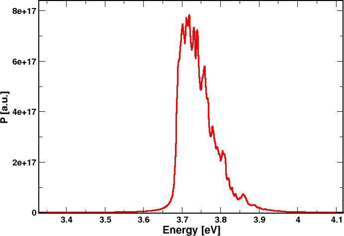
We find the following emission spectrum, showing an emission peak at the fundamental transition energy.


